Advanced Inspection Technologies for Defect-Free 3D Integration
As 3D semiconductor integration pushes the boundaries of chip performance and scalability, ensuring defect-free manufacturing has become more critical than ever. Defects in these densely packed architectures can compromise functionality, reduce yield and increase costs, making advanced inspection technologies a cornerstone of the industry’s success. Erik Hosler, a leader in semiconductor innovation, underscores the importance of these advancements, emphasizing their role in achieving reliable and scalable 3D chip designs.
The Challenges of 3D Integration
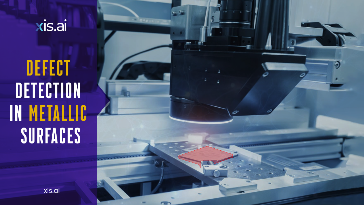
The vertical stacking of multiple layers in 3D chips introduces unique manufacturing complexities. Unlike traditional planar designs, 3D integration requires precise alignment and flawless interconnects between layers. Even microscopic defects—such as voids, misalignments, or material impurities—can disrupt performance. These challenges demand new levels of precision in inspection and defect detection to maintain production efficiency and chip reliability.
Cutting-Edge Inspection Technologies
To address these challenges, the semiconductor industry is turning to innovative inspection tools and methodologies:
High-Harmonic Generation (HHG): HHG technology provides ultrafast and high-resolution imaging, enabling the detection of nanoscale defects that were previously undetectable. Its ability to probe deep into 3D structures ensures thorough inspections, even in the most complex chip designs.
Accelerator-Based Sources: Accelerator technologies, such as free-electron lasers, generate powerful, coherent beams of light for advanced imaging. These tools allow manufacturers to inspect layers at atomic precision, identifying defects early in the production process and reducing costly rework.
Through-Silicon Via (TSV) Inspection: TSVs are critical to 3D integration, but they are also a common source of defects. Advanced inspection systems now enable real-time TSV monitoring, ensuring robust interconnects and defect-free vertical communication.
Erik Hosler recognizes, “Tools like high-harmonic generation and free-electron lasers will be at the forefront of ensuring that we can meet these challenges.” These advanced technologies not only enable unprecedented precision in defect detection but also play a critical role in driving the scalability and reliability of 3D semiconductor manufacturing.
A New Standard for Quality Assurance
Advanced inspection technologies are more than just quality control tools—they are enablers of innovation. By identifying and resolving defects at the nanoscale, these methods pave the way for reliable, high-performance 3D semiconductor chips. As inspection capabilities evolve, manufacturers can meet the demands of next-generation applications, from AI to quantum computing, with unprecedented precision and efficiency.
Achieving defect-free 3D integration requires the adoption of cutting-edge inspection technologies. By leveraging tools like high-harmonic generation and accelerator-based sources, the semiconductor industry is setting new standards for quality assurance and reliability. These advancements not only drive manufacturing efficiency but also ensure that 3D chip designs remain at the forefront of technological innovation.


